So dynamic IR drop will be addressed. Power planning means to provide power to the every macros standard cells and all other cells are present in the design.
Ir Drop Issue In Vlsi What Is Ir Drop In Asic Why Ir Drop Effects Of Ir Drop Youtube
What are the different types of delay models.

. IR core 775 mV IR package IR pads 5 To determine values for IRpackage and IRpads consider that IRpackage consists of. Not only can timing change but it can directly cause functional failures. A WLM wire load model b NLDM non linear delay.
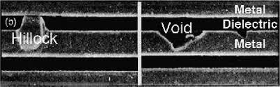
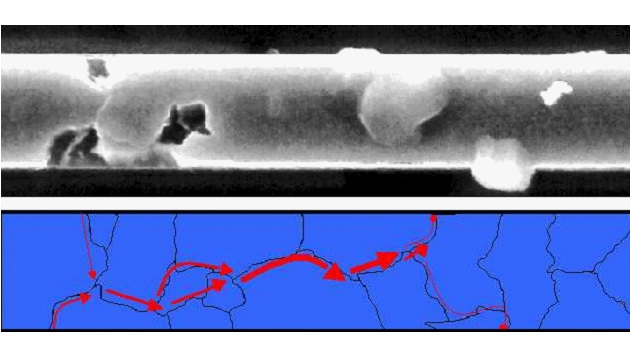
I had 5 clocks in my designs sys_clk sys_rclk uart_clk g_clk and scan_clk where sys_clk g_clk and uart_clk logically exclusive to scan_clk. 250 Physical Design Engineer Interview Questions and Answers Question1. As the dimension of integrated circuit were progressively reduces current density flowing through the particular metal increases eventually exhibit open circuit of.
IR drop while causing an increase in delay for a digital transistor can have an even bigger impact on analog circuitry. 5 Real Reasons Why More People Are Increasingly Opting for Physical Design Training. Power requirement of the design Power network structure.
Why power stripes routed in the top metal layers. Industry standard Project Execution 1. The delay changes and the reduced supply voltage of the cells in turn affect power consumption in the design.
A physical design process to determine if chip satisfies rules defined by the semiconductor manufacturer. RAS Lecture 6 16 Reducing the Effects of IR drop and Ldidt Stagger the firing of buffers bad idea. Caused by cell currents.
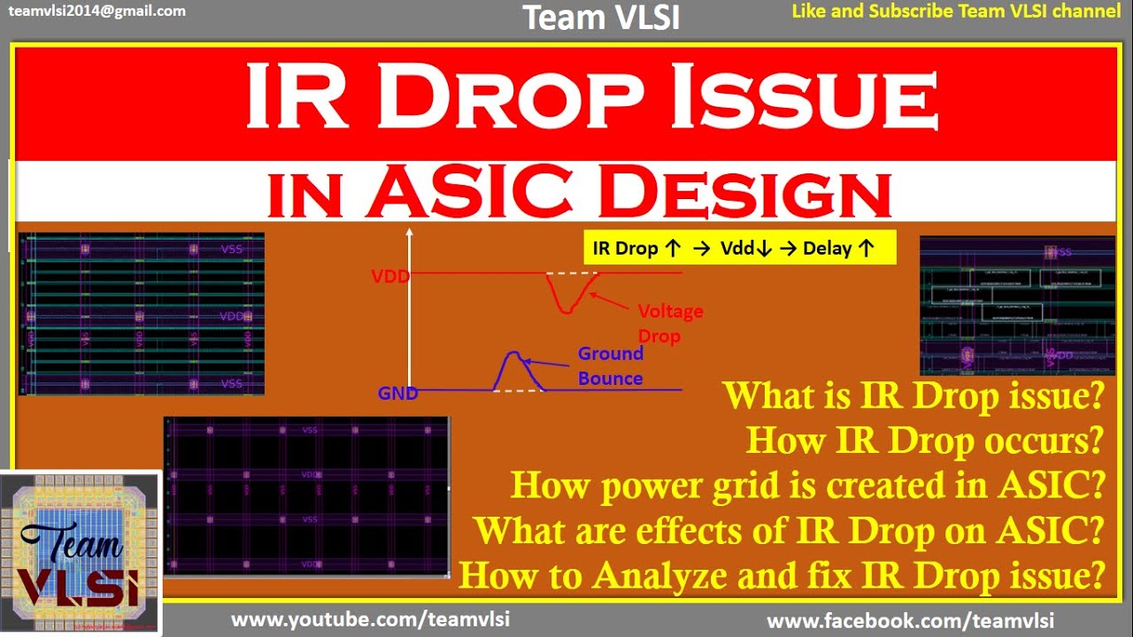
IR Drop Analysis IR Drop. In this create power and ground structure for both IO pads and core logic. Increases skew Use different power grid tap points for clock buffers but it makes routing more complicated for automated tools.
Load splitting can reduce the peak current demand from the power grid. The voltage that gets to the internal circuitry is less than that applied to the chip since every metal layer offers resistance to the flow of current When a current I passes through a conductor with resistor R it exhibits a voltage drop V which is equal to the resistance times the current. Amount of current drawn from the power grid is directly proportional to the output capacitance thats being driven.
As the VLSI industry continues to expand more people are opting for training in the area of the. At 5nm a very strong increase in both electrical and thermal parasitics is expected Dr. Package cross-section showing IR drop components Combining 3 4 and the value for IR chip found in 2 provides a formula for determining an actionable IR drop target for the physical design process.
VLSI Physical Design Data preparation import design floorplan Power planing power ring core power IO power ring pad bump creattion. Typically power consumption is lower when IR-drop effects are considered. Answer 1 of 3.
D Physical information of the design. The IO pads power and ground buses are built into the pad itself and. Physical information of the design report_design_physical Digital Signal Processing Tutorial.
Christoph Sohrmann advanced physical verification at Fraunhofer Institute for Integrated Circuits IIS said. How Many Clocks You Had In Your Designs. An IR drop on the power and ground rails affects cell delaysthe higher the IR drop the slower signal changes propagate through cells.
The netlist is the logical description of the ASIC design. Effects of IR-Drop on Clock Skew Without IR-drop With IR-drop Plots courtesy of Simplex Solutions Inc. Power and Ground nets are usually laid out on the metal layers.
Top metal layers are thicker and offer lesser resistance. This helps to reduce IR drop. Floorplanning is the process of placing blocksmacros in the chipcore areaIn this step we have netlist which describes the design and the various blocks of the design and the interconnection between the different blocks.
Vlsi pnr cts physicaldesign mtech cadence synopsys mentor placement floorplan routing signoff asic lec timing primetime ir electromigratio. The major stages are explained below. Floorplanning is the most important process in Physical Design.
Industry Standard Physical Design Live Project. IR Drop and EM Analysis IR Drop Drop happens in supply voltage when traverses through the power network. I have used both Cadence and Synopsys tools extensively so those are what I will base my examples on.
It is one of the failure mechanism encountered in high density logic. In order to reduce effect of IR drop we need to make these routes less resistive. IR Drop analysis Static and Dynamic.
The first stage in physical design flow is reading in the netlist and the constraints to your tool of choice. How Did You Do Cts For The Same. B Allowable IR drop.
Why metal density rules are important. Design Rule Pattern Matching. Let us see what kinds of files we are dealing with here.
C Global route congestion. First of all the FinFET design will suffer from stronger self-heating. However decaps are leaky and it will add to the leakage power in the design Splitting output capacitance.
Understanding Electromigration And Ir Drop In Semiconductor Chip Design Challenges And Techniques Ele Times

Vlsi Basics Electromigration Ir Drop

Tutorial Ir Drop Analysis Lower Technology Node Physical Design Asic Electronics Vlsifab Youtube
Understanding Electromigration And Ir Drop In Semiconductor Chip Design Challenges And Techniques Ele Times
Understanding Electromigration And Ir Drop In Semiconductor Chip Design Challenges And Techniques Ele Times

Ir Drop Issue In Vlsi What Is Ir Drop In Asic Why Ir Drop Effects Of Ir Drop Youtube
Tutorial Ir Drop Analysis Lower Technology Node Physical Design Asic Electronics Vlsifab Youtube
Understanding Electromigration And Ir Drop In Semiconductor Chip Design Challenges And Techniques Ele Times
0 komentar
Posting Komentar